join us in upcoming EVEntS
Upcoming Workshops (Singapore)
Workshops for learning
For more details of the workshops, pls sent email to admin@launchxtec.com
Venue: Newcastle Australia Institute of Higher Education Singapore, 230 Victoria Street, #04-09/10, Bugis Junction Towers, S188024
Registration fee: SGD 800 per workshop (3 weeks before the workshop) and SGD 1,000 per workshop thereafter. We are pleased to offer the following discounts for block booking:
10% discount for registering for 3–5 workshops (any combination)
15% discount for registering for >5 workshops (any combination)
Please request a quotation by emailing admin@launchxtec or proceed with registration and payment via PayNow.

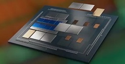
Advanced Package Assembly Technologies and Performance Engineering in Heterogeneous Integration
(12-13 Mar)
This workshop provides a comprehensive introduction to advanced packaging technologies, beginning with the critical role of IC packaging in enabling compact, high-performance, and application-driven electronic systems. It compares System-in-Package (SiP) and System-on-Chip (SoC) approaches across key markets including wireless, computing, power, and automotive applications.
Participants develop a foundation in thermal and electrical management, covering heat transfer principles, thermal modelling, signal integrity and noise mechanisms essential to reliable high-speed designs. The workshop then explores interconnect technologies, board-level assembly, and soldering processes, with a focus on Pb-free materials and reliability considerations. The program concludes with an in-depth review of package assembly technologies, spanning wafer thinning, stealth and plasma dicing technologies, die attach, compression molding, plating, and singulation. This workshop is designed to help engineers rapidly build practical knowledge of state-of-the-art package assembly technologies, materials, and industry best practices
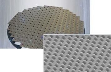


Wafer-Level Packaging and C4 Flip Chip Interconnects for Advanced Semiconductor Integration
(26-27 Mar)
This intensive two-day workshop delivers a detailed yet practical overview of C4 Flip Chip and Wafer-Level Packaging (WLP) technologies, with emphasis on the materials, process integration, and reliability challenges that enable high-density, high-performance semiconductor systems. Participants will explore heterogeneous integration trends, wafer-level interconnect fundamentals, and the evolution of Redistribution Layer (RDL) and Underbump Metallization (UBM) architectures that support fine-pitch C4 assemblies. The workshop covers wafer bumping and lead-free solder technologies, multiple bonding mechanisms including C4, thermocompression, and solid-state bonding, and critical design considerations for wafer-level integration. It concludes with in-depth discussion of characterization and reliability evaluation methods—such as interfacial analysis, failure mechanisms, temperature cycling, thermal shock, and moisture sensitivity—providing engineers with the knowledge to design, manufacture, and qualify reliable C4 flip chip and WLP solutions.
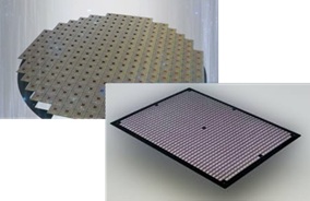
Breaking Down Panel level & Fan-out Wafer-Level Packaging: Design, Assembly, and Competitive Technologies
(16-17 Apr 2026)
This workshop provides a comprehensive overview of chiplet-based and heterogeneous integration technologies, starting with IC packaging fundamentals, key market and technology drivers, and the industry shift from monolithic SoC toward modular SiP and chiplet architectures to enable scalability, performance, and design flexibility. It introduces Wafer Level Packaging with a focus on the limitations of Fan-In WLP and the advantages, evolution, and industry adoption of Fan-Out WLP as a critical enabler for high-density integration. Participants then explore wafer-level and panel-level FO-WLP through die-first and die-last architectures, real-world case studies from leading vendors, key assembly and reliability challenges, and future scaling toward PoP and panel-level manufacturing. The workshop concludes with an examination of emerging and competing technologies for advanced chiplet systems, including next-generation substrates, multi-dimensional packaging concepts, hybrid bonding, and glass core substrates, offering a forward-looking perspective on the future of advanced semiconductor packaging.
👉 Register now for Mar - Apr through the link below to secure your spot:

For workshop details, pls refer to the link
https://docs.google.com/document/d/1n6JRpFh82iZ5oLc5AjOrxEnz0V8QqMDAHWF9aZ1J7VI/edit?usp=sharing
For workshop details, pls refer to the link
https://docs.google.com/document/d/1a5kwkT4nNvO5meshyvqKIBojhV5NEaaA6s3kUK5zXl0/edit?usp=sharing
For workshop details, pls refer to the link
https://docs.google.com/document/d/13eaRh8dpxG91zH4i_uZwh9ROs9efaWkA6xmFlBioj1k/edit?usp=sharing